Semiconductor Equipment: Enabling Advancements in Today's Technology

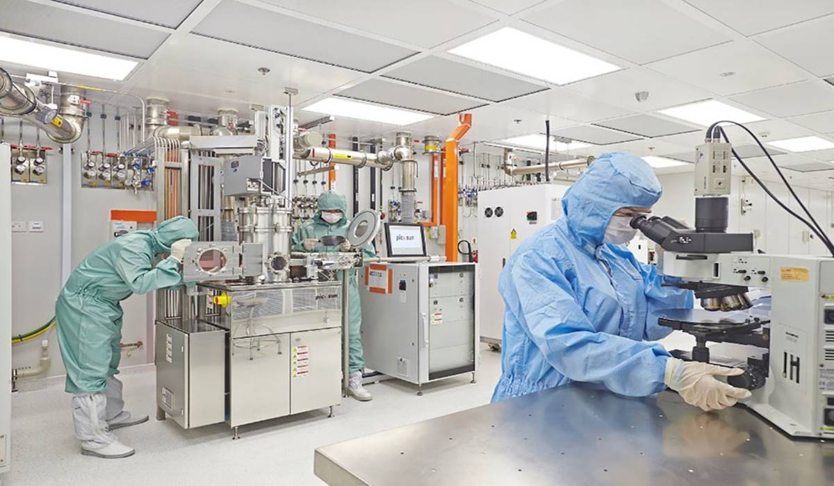
The semiconductor industry plays a vital role in powering today's technology. From smartphones and computers to appliances and vehicles, semiconductors are embedded in nearly every electronic device we use on a daily basis. Continued advancements in semiconductor technology have allowed for improvements in performance, power consumption, size and cost—driving further innovation. However, the manufacturing of semiconductors would not be possible without specialized semiconductor equipment. This multi-billion dollar industry develops and produces the tools necessary for the fabrication of integrated circuits.
Lithography Machines - Driving Miniaturization
As transistors continue shrinking to enable more powerful yet efficient chips, lithography machines remain at the forefront of semiconductor manufacturing. These complex systems are used to transfer circuit patterns onto silicon wafers. Advances in lithography have allowed feature sizes to decrease from tens of micrometers in the 1970s to just a few nanometers today. The latest extreme ultraviolet (EUV) lithography tools can print lines as small as 7 nanometers, enabling over 20 billion transistors to fit on a cutting-edge chip. Looking ahead, the industry is working towards the 5 nanometer node and beyond through continual enhancements in EUV performance, resolution and throughput.
Deposition and Etching Systems - Layer by Layer Fabrication
After circuit patterns are defined using lithography, several deposition and etching steps are required to build up the multi-layered structure of an integrated circuit. Deposition tools such as chemical vapor deposition (CVD) and physical vapor deposition (PVD) deposit thin films of various materials including silicon, dielectrics, and metals. Meanwhile, plasma and reactive ion etching tools selectively remove deposited films to transfer patterns onto underlying layers. Continuous improvements in processes like atomic layer deposition (ALD) have made it possible to deposit ever thinner yet highly conformal layers with unprecedented control at the atomic scale. These types of equipment play a crucial role in advancing Moore's Law and 3D chip architectures.
Process Diagnostics and Control - Enabling Quality and Yield Management
Given the complexity of today's chip manufacturing processes involving hundreds of steps, process diagnostics and control equipment have become equally sophisticated. Systems like optical emission spectroscopy, electron beam inspection and metrology tools carefully monitor critical dimensions, film thicknesses, contamination levels and more. They provide real-time data for fault detection and run-to-run control to help maximize product quality and yields. Advanced data analytics is also being leveraged to correlate equipment performance with downstream results. As process windows continue shrinking with each new technology node, precise in-line controls will remain essential for high-volume production.
Packaging and Assembly Technologies - Meeting Industry Demands
Once individual chips or dies are manufactured, they must be assembled into complete packages and modules through multi-step packaging and assembly processes. Dedicated equipment is required for tasks such as die bonding, wire bonding, molding, bumping, testing and more. 3D and advanced packaging technologies especially require new innovations, as structures become more complex with Through-Silicon Vias, stacks of dies and alternative interconnections. In addition, trends like artificial intelligence, autonomous vehicles and the Internet of Things driving demand for heterogenous integration of different chips (memory, logic, analog, RF, MEMS, etc.) in a single package. Equipment suppliers continue advancing their technologies to support these rapidly evolving packaging needs.
Market Outlook and Advancements
The semiconductor equipment market currently stands over $60 billion globally and is forecasted to experience steady growth in coming years according to various analysts. Many companies are actively developing new systems that can support upcoming nodes with EUV lithography, as well as enabling technologies like Multi-Beam e-beam direct write lithography and extreme ultrafast lasers. There is also significant focus on addressing industry megatrends through new assembly and metrology solutions. Looking further ahead, disruptive lithography concepts beyond EUV such as extreme ultraviolet free electron lasers and nanophotonics are under research. Overall, continued R&D investment will be crucial for the semiconductor equipment industry to maintain Moore's Law and power advancements in logic, memory, sensors and other market segments that are core to digital transformation.
Specialized Semiconductor Equipment plays an indispensible role in the multi-billion dollar semiconductor industry. Continuous innovations across lithography, deposition, etching, metrology, packaging and other areas have allowed semiconductor feature sizes to shrink each generation according to Moore's Law. This scaling has enabled ever more powerful yet efficient chips that fuel technologies impacting nearly every aspect of modern life. Going forward, focused R&D will be important for the equipment industry to support emerging developments in areas like EUV lithography, heterogenous integration, 3D stacking and new computing paradigms. Their efforts will drive further advancements across industries relying on semiconductors for ongoing digital transformation.
Explore more information on this topic, Please visit -
https://www.newswirestats.com/semiconductor-equipment-market-share-and-demand-analysis/